
Key Features
- Internally matched GaN MMIC PA
- Frequency Range8 to 12 GHz
- Small Signal Gain32dB
- 21dB Power Gain with Pin = +22dBm
- PAE42% with +22dBm Pin
- Output Power17W
- Quiescent Bias+28V @ 200mA
- Compact Size5x5 mm
Applications
- Weather & Marine Radar
- Test & Measurement
- X-Band Transceivers
- EW / ECM / C-UAS
Architecture
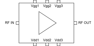
ATEK581N5 Block Diagram
ATEK581N5 is a GaN MMIC high-power 17W amplifier operating from 8 to 12 GHz while providing 32dB of small signal gain.The ATEK581N5 delivers +42dBm output with 42% power added efficiency over the 8 to 12GHz band.The power amplifier is housed in a compact 5x5mm SMD package with input and output matched to 50 ohms internally.Evaluation Board, custom package, and module options are available upon request.
Technical Specifications
| Parameter | Condition | Min | Typical | Max | Unit |
|---|---|---|---|---|---|
| Frequency Range | 8 | 12 | GHz | ||
| Output Power (Pin: +22 dBm) | 8 GHz | 42.9 | dBm | ||
| 9 GHz | 43 | dBm | |||
| 10 GHz | 42.7 | dBm | |||
| 11 GHz | 42.6 | dBm | |||
| 12 GHz | 42.3 | dBm | |||
| Small Signal Gain | 8 GHz | 31.7 | dB | ||
| 9 GHz | 32.1 | dB | |||
| 10 GHz | 32.1 | dB | |||
| 11 GHz | 31.5 | dB | |||
| 12 GHz | 32.3 | dB | |||
| Input Return Loss | -17 | dB | |||
| Output Return Loss | -12 | dB | |||
| Noise Figure | TBD | dB | |||
| Output IP3 | TBD | dBm | |||
| Drain Voltage (Vdd1, Vdd2, Vdd3) | 24 | 28 | 32 | V | |
| Gate Voltage (Vgg1, Vgg2, Vgg3 Adjust the gate voltage between -4V and -1V to achieve an IDQ = 200mA typical) | -2.1 | V | |||
| Quiescent Current (Idq1 + Idq2 + Idq3) | 200 | mA | |||
| PAE | 42 | % | |||
| Operating Temperature | -40 | 85 | °C |
Available Resources
Ready to Integrate ATEK581N5?
Contact our engineering team for technical support, samples, or volume pricing.